
 Case Details
 F3F TIMER PROJECT by Jon Edison
Updated May 2022
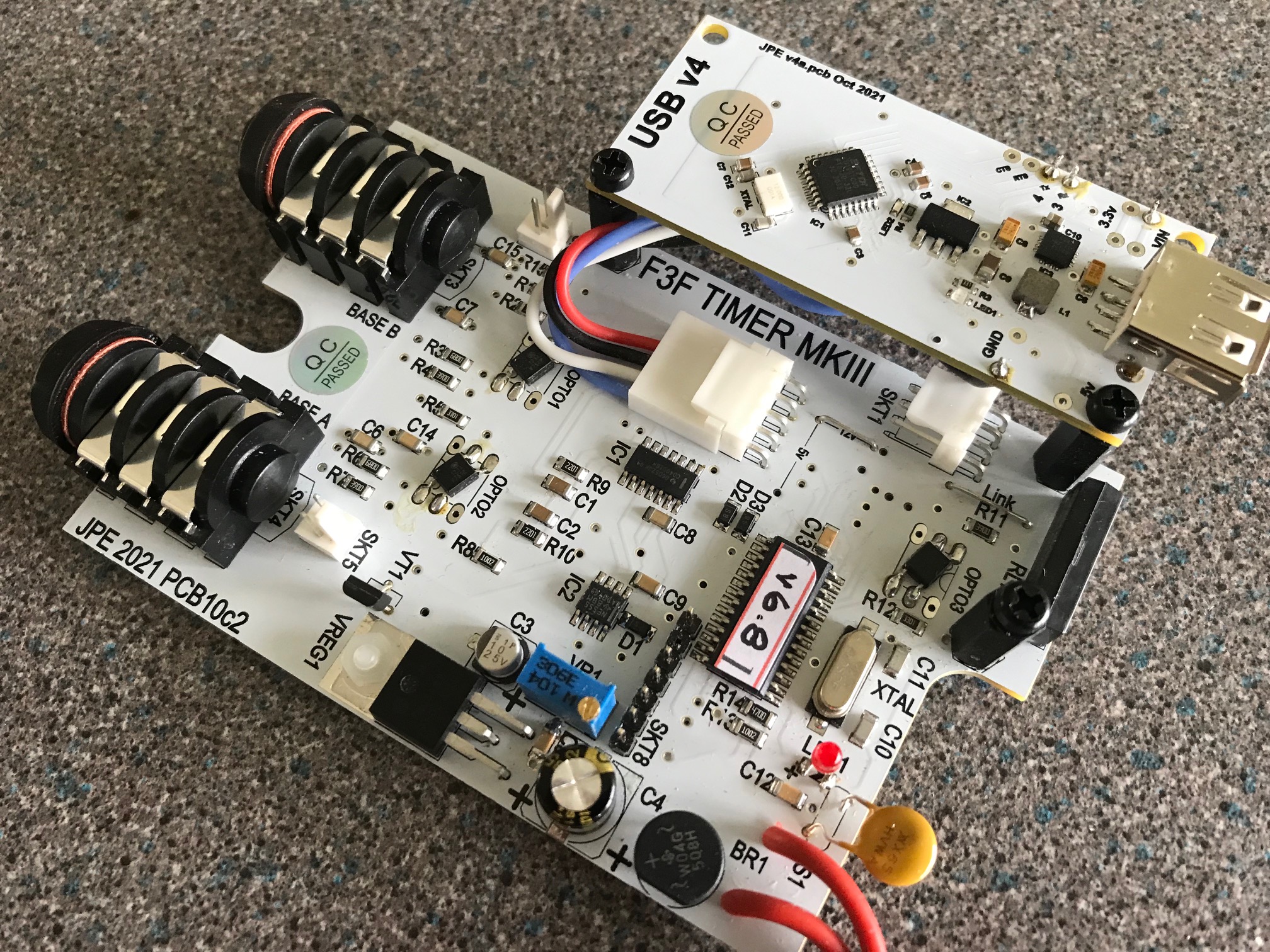
MK III Construction Details
< Back ( Additional Components ) Next >
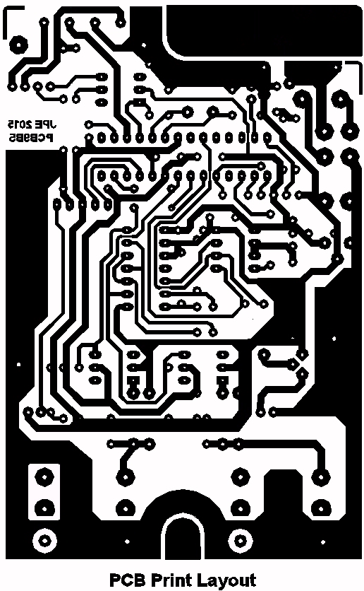
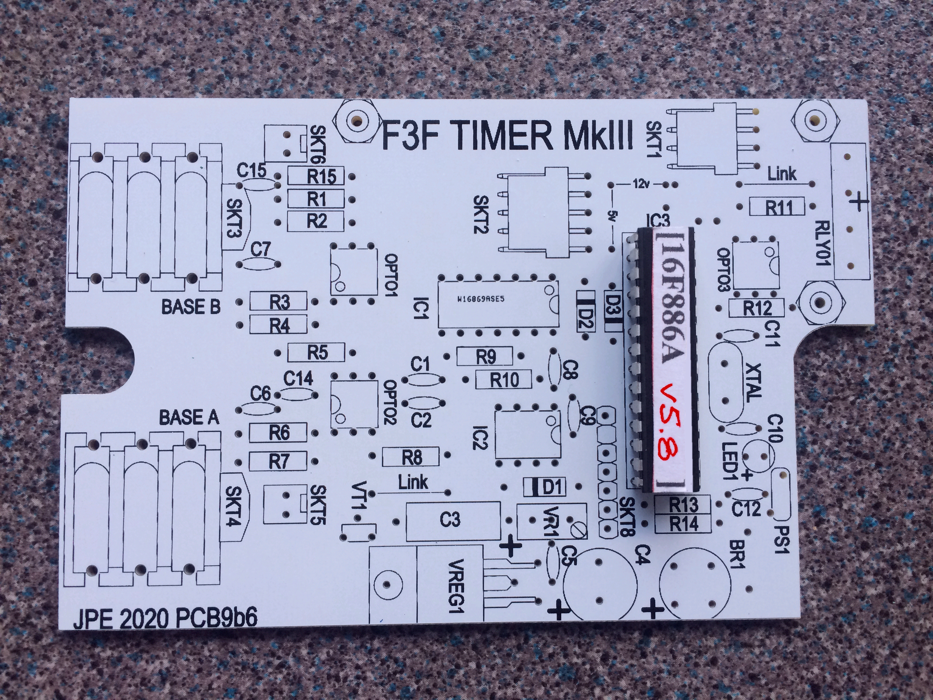
Both the PCB design and Component Layouts are shown below.
The PCB is
shown Full Size.
This design allows for easy home construction as all the components are 'through hole' mounted. Components are available from suppliers such as Rapid Electronics, RS Components, Technobots etc.
A pre-programmed processor ( IC3 ) and professionally manufactured Printed Circuit Board ( PCB ) for home construction, are available from the author for £35.
An fully assembled and tested PCB complete with USB interface, is available for £220. If it is required to have the PCB installed in a IP42 case, then this can be added for an additional £30
PCB
Produce the PCB using a photo etch process. Drill all holes 0.8mm. Open up the holes shown in red to 1.0mm. Blue holes to 1.3mm, and Green holes to 3mm.
PCB Assembly
Start with C13 and the Link under IC3. Make sure C13 is as close to the pcb as possible. Install the 28pin DIL socket over the link and C13.Then install the remaining larger components such as BR1, C4, VREG1, OPTO1, 2, and 3, IC1 and IC2. These give a guide to the positions for the remaining Resistors, Capacitors and Diodes. Finish off with the Molex and other components . Finally, mount IC3
New SMD PCB Components
in the 28pin DIL Socket.
PCB Testing
Check and check again that there are no solder bridges between tracks, and all IC's and Diodes are the correct way round. Wire sockets SKT10 and 11 to the board with short lengths of cable. Check with a multimeter that no short exists on the board by placing the meter set to continuity / resistance across these sockets. If all is well, a reading greater than 500K ohm will be obtained. Now set the multimeter to its Current setting and place the meter inline with one of the input wires. Apply a voltage of between 9 and 12 volts to the board via the multimeter, a reading of approx 30mA ( 60mA if the IOIO board is attached ) will be shown, and LED1 will be lit. Recheck if readings are seriously higher than these. Otherwise you have successfully produced a working timer which can now be mounted in its case.
Case
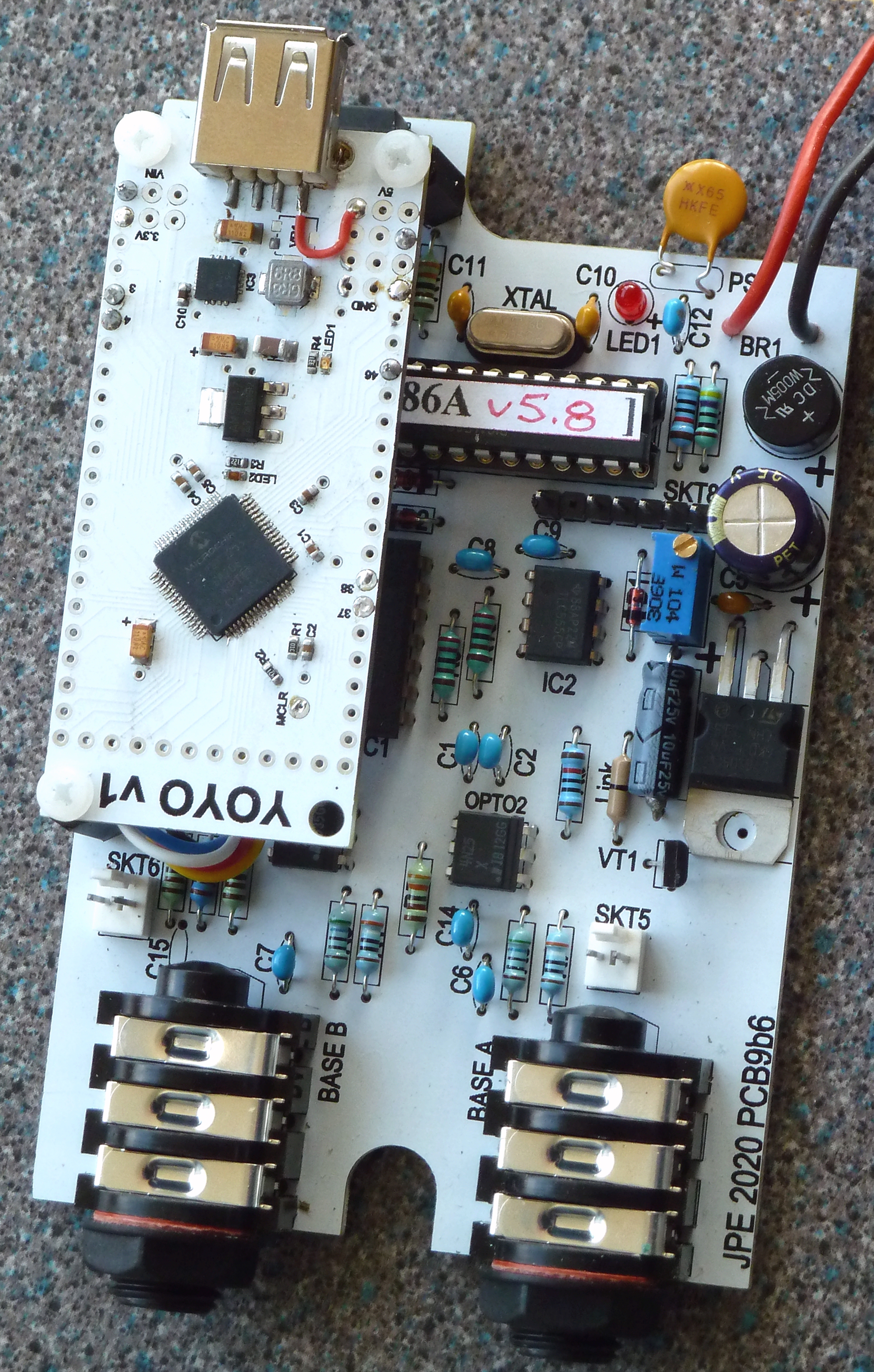
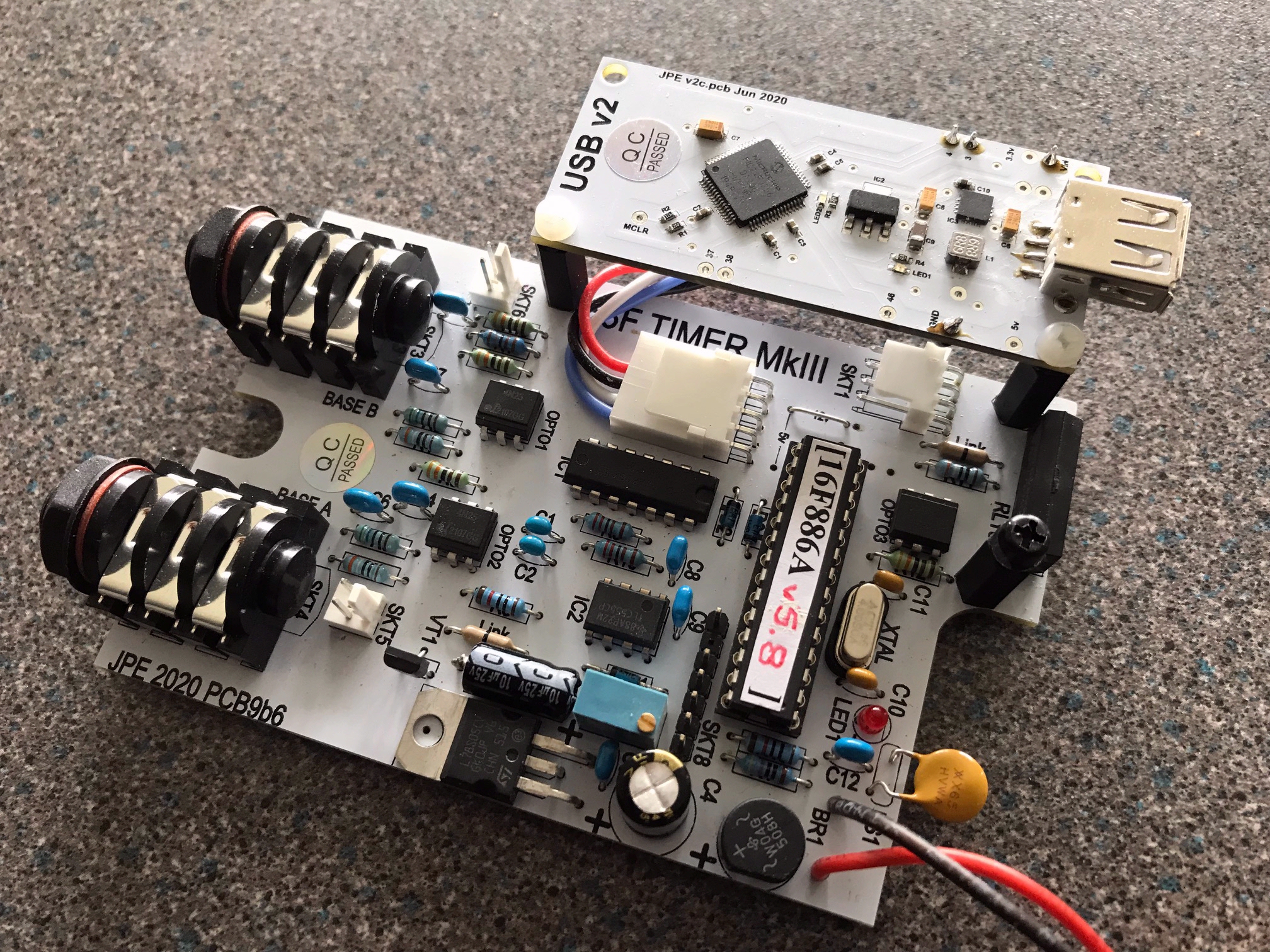
Drill the case as shown. The PCB is designed to be held in position by SKT3 and 4. After testing, slip the board into the case, sockets first, then tighten the two nuts on the sockets to securely hold the board. Mount SKT10 and 11, and connect to the board. Install and connect Sockets SKT7 and SKT9. Finally connect the IOIO board to the main pcb, and mount on the 3 nylon pillars. NB the IOIO board shown is the recommended V1 board. Later versions have a smaller USB connector.
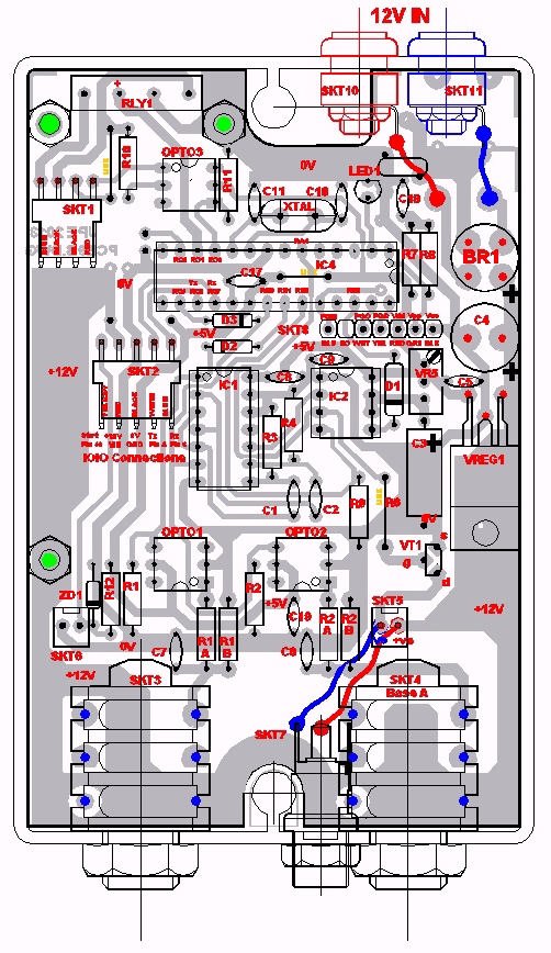 Component Layout
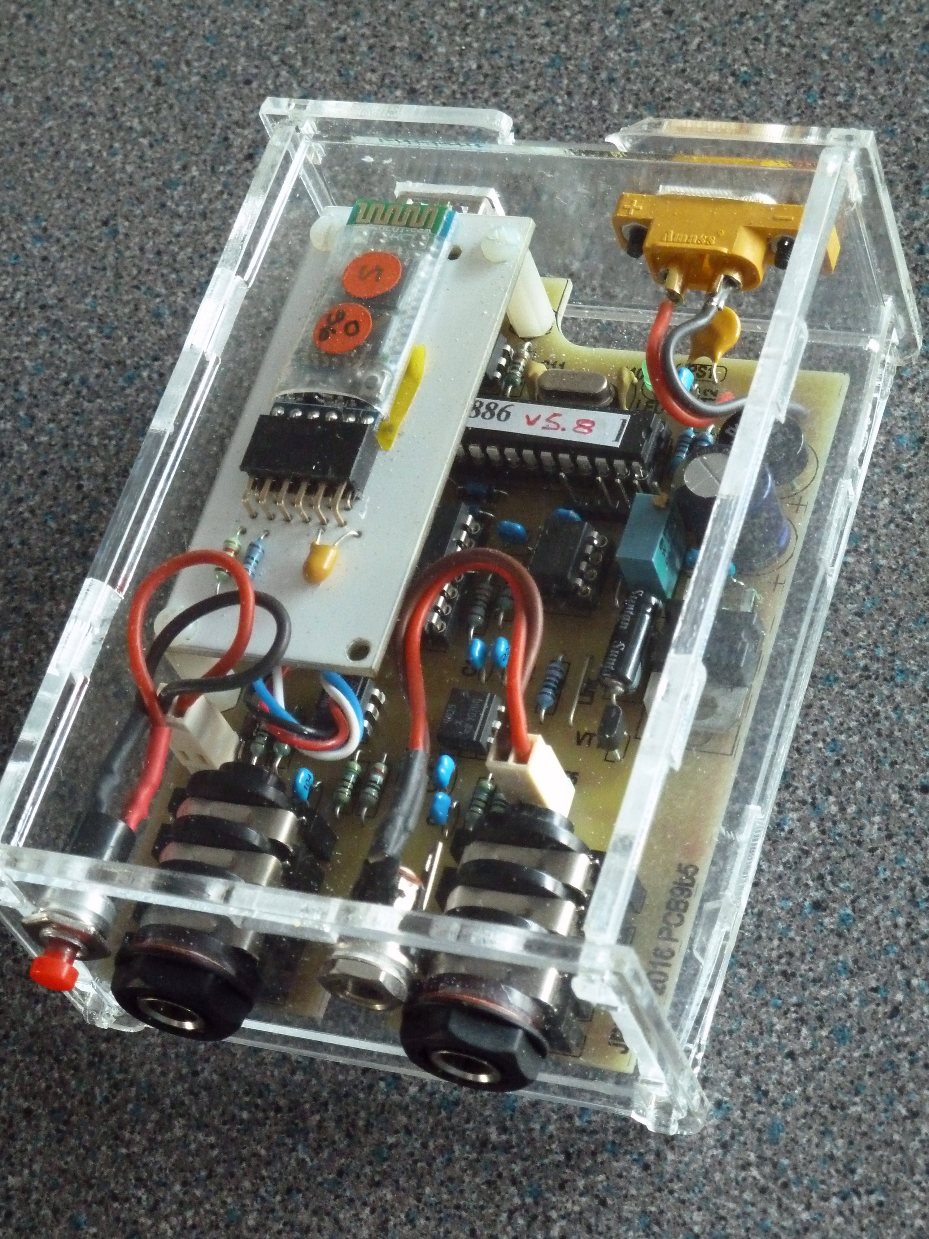
PCB in Show Case
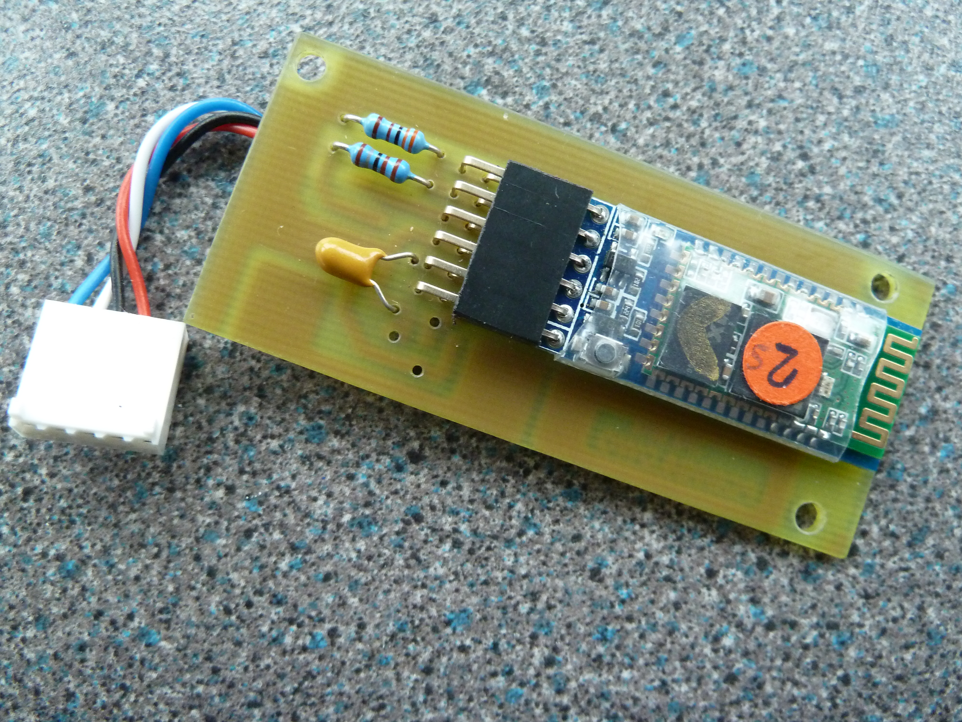 Bluetooth HC-05 Module
Jon Edison
May 2015. Updated May 2022.
New SMD PCB under Development
Disclaimer
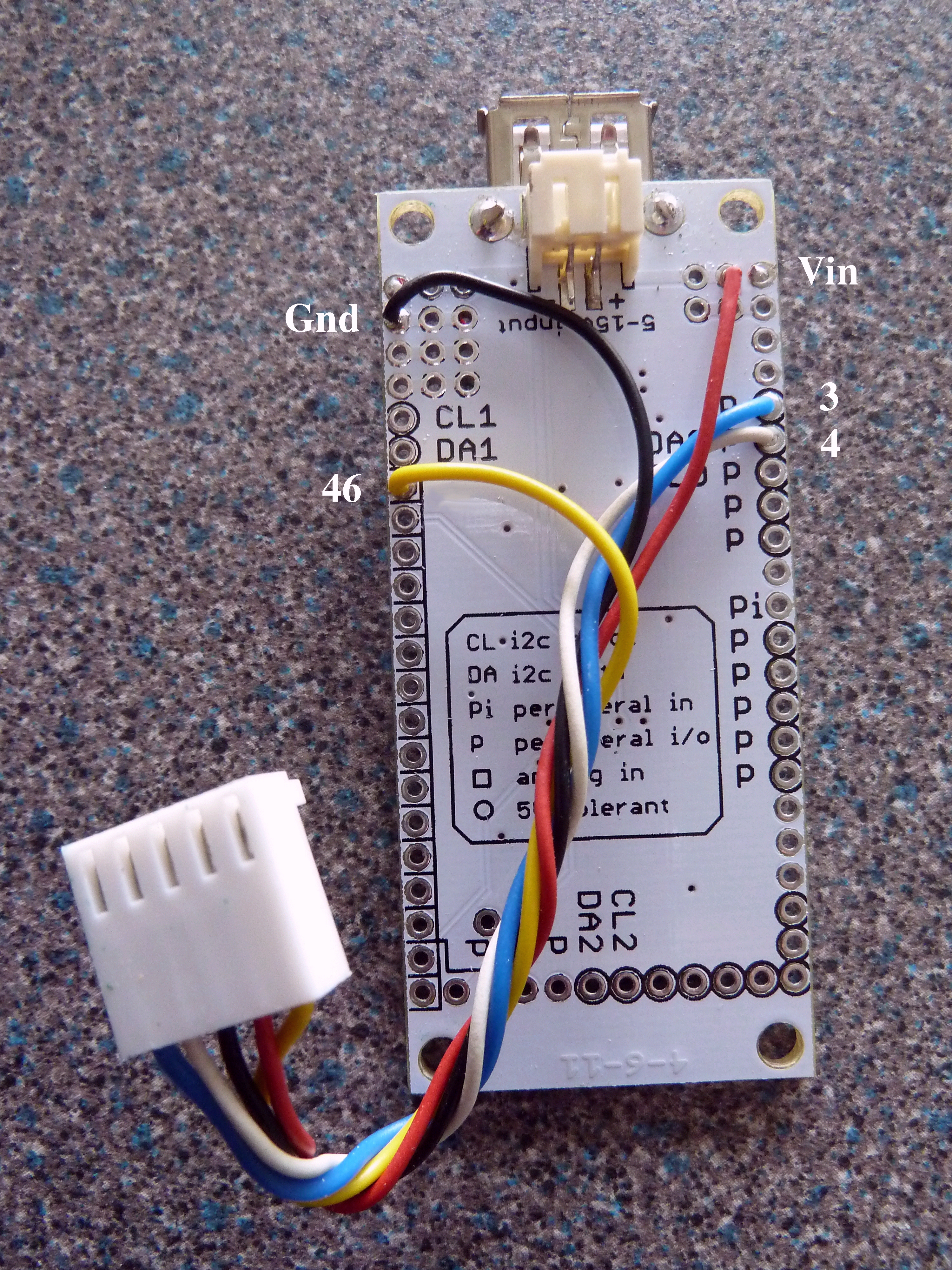 IOIO Connections
I have no connection with any of the companies listed, any links given are for information only, and for use at your own risk. All information is given in good faith and without liability.
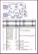
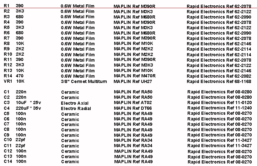 Component
List